The LTELink project is a custom carrier board designed for the Radxa CM3, aimed at creating a compact, high-performance communications hub featuring LTE connectivity and a built-in Ethernet switch.
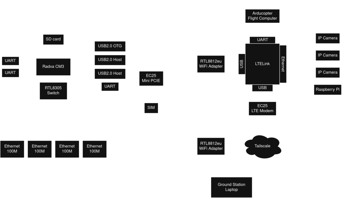
Block diagram of the PCB (left) and of its connectivity (right)
Phase 1: The Blueprint (November 2025)
The journey began with a focus on high-density integration. The core goal was to combine a Quectel EC25 LTE modem (via MiniPCIE) with an RTL8305 5-port 100M Ethernet switch.
-
Ethernet Strategy: A 100M switch was chosen over Gigabit to simplify routing (two pairs vs. four) while still providing more than enough bandwidth for multiple 1080p video streams.
-
USB Innovation: Rather than adding a dedicated micro-USB port for programming, a unique manual jumper system was designed to toggle the USB-C port between Power/OTG and Host modes.
-
Layering: The design utilized a 4-layer stackup to manage controlled impedance for high-speed signals.
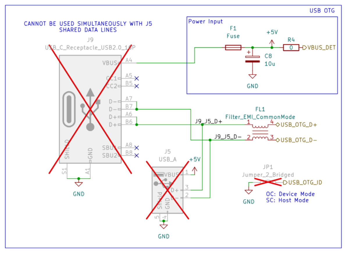
Mechanism for toggling between OTG on the USB-C port and host mode on the USB-A port
Phase 2: Power and Precision (Early February 2026)
As the design matured, the focus shifted to power stability and flight-controller integration.
-
Dedicated Power: Realizing the LTE modem can pull up to 2A, a powerful 5V-to-3.3V converter was added to ensure stable operation.
-
MAVLink Integration: Three UARTs were wire, with one specifically for MAVLink connections, positioning the board as a powerful companion for drone telemetry and video.
-
Layout Refinement: The area around the RTL8305 was optimized for filtering components, and the MiniPCIE connector was swapped for a taller version to clear the SIM card slot.
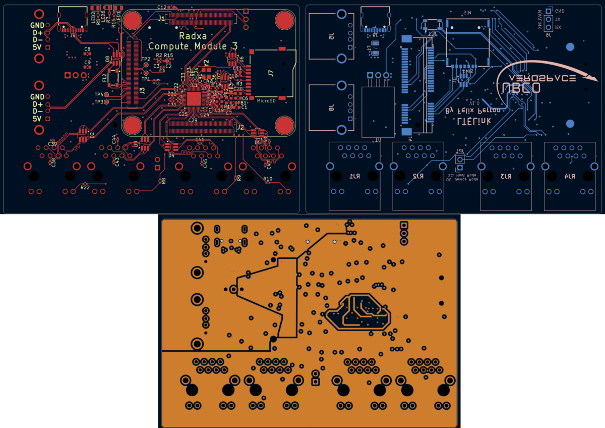
Layout of the top (red), bottom (blue) and power (orange) layers
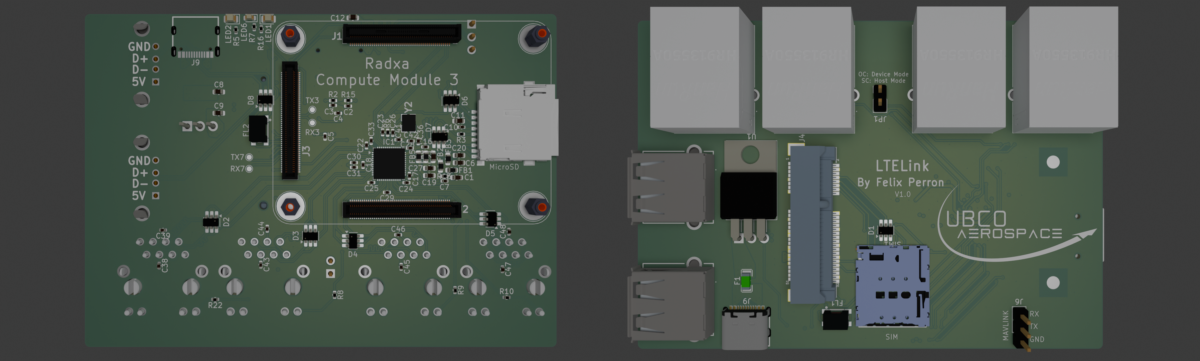
Render of the top (left) and bottom (right)
Phase 3: Crisis Management & Success (Late February 2026)
The first hardware arrival brought a major challenge: a mirrored footprint for the middle Radxa CM3 connector (J3). This would typically mean a dead board, but some "surgical" persistence saved the prototype.
Hardware "Quick-Fixes"
| Issue | Workaround Performed |
| J3 Footprint Mirrored | Manually cut traces and soldered wires to tiny 0.2mm pins. |
| USB_VBUS_DET Level | Manually wired the pin to 3.3V instead of 5V. |
| LED Polarity | Rotated status LEDs 180° by hand. |
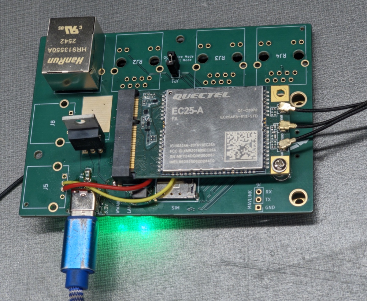
Functional prototype after manual fixes
The Software Breakthrough
Despite the hardware hurdles, the software side saw massive wins. After modifying the Debian device tree to remove missing hardware, the board successfully:
- Booted the OS and connected to Wi-Fi.
- Verified the RTL8305 Ethernet switch worked flawlessly.
- Established an LTE connection via Tailscale, enabling live video streaming over a cellular network.
What’s Next?
While the current board is a "Frankenstein" of jumper wires, it has proven the concept works. The next steps involve:
-
Updating the design files to fix the mirrored footprint and serial conflicts.
-
Ordering a second (and hopefully final) revision of the PCB.
-
Exploring Buildroot for a more lightweight, optimized OS.